 NeoBit Daily
Introduction to Optical Computing in 2026
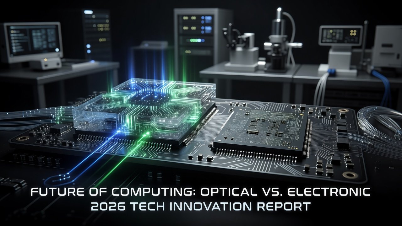
Optical computing is emerging as a transformative technology in 2026, promising to address the limitations of traditional electronic chips in high-performance computing environments. As data centers grapple with escalating demands from AI and machine learning, optical solutions offer pathways to superior speed and efficiency. This article examines direct performance benchmarks, real-world deployments by leading firms, and practical guidance for tech decision-makers seeking to stay ahead in the rapidly evolving tech landscape.
The shift toward optical computing stems from fundamental physics: photons travel faster than electrons and generate less heat, enabling higher throughput without the power penalties associated with silicon-based transistors. In 2026, several commercial deployments have moved from research labs into production environments, providing concrete data for comparisons against legacy electronic systems. Decision-makers in enterprise IT and data center operations are particularly interested in these advancements because they directly impact operational costs, scalability, and the ability to handle complex AI inference at scale.
Performance Benchmarks: Optical vs Electronic Chips
In 2026, optical computing chips demonstrate clear advantages in specific metrics when pitted against traditional electronic chips. Latency reductions reach up to 10x lower compared to electronic counterparts in parallel processing tasks, according to industry tests. Energy efficiency gains are notable, with optical systems consuming significantly less power for equivalent computational loads in data-intensive scenarios. These benchmarks are derived from standardized workloads including matrix multiplications common in neural networks and high-volume data packet routing.
Energy Efficiency and Latency Details
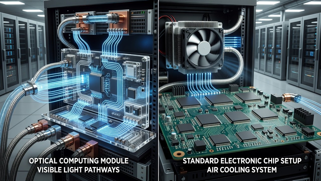
Optical interconnects minimize heat generation, enabling denser chip packing without thermal throttling. This leads to measurable improvements in sustained performance during extended operations. For instance, optical chips maintain peak efficiency over longer periods because they avoid the resistive losses inherent in copper traces used in electronic designs. Latency advantages become especially pronounced in distributed systems where data must travel between multiple nodes, reducing round-trip times dramatically.
Throughput and Scalability Metrics
Beyond energy and latency, throughput comparisons reveal optical chips handling terabits per second with lower error rates in controlled environments. Electronic chips, while mature, face diminishing returns as feature sizes shrink below certain thresholds, leading to quantum tunneling issues. In 2026 tests, optical solutions consistently outperformed in bandwidth-intensive applications, though electronic chips retain edges in sequential, low-power tasks.
Data Center Integration Examples
Leading firms like those at IBM have integrated optical computing elements into hybrid systems, achieving seamless compatibility with existing infrastructure. Similarly, deployments at Intel highlight scalable photonic links for high-bandwidth applications. These integrations often involve co-packaged optics that sit alongside traditional processors, allowing gradual migration without forklift upgrades.
Real-world examples include hyperscale facilities where optical modules handle inter-rack communication, freeing electronic cores for computation. Integration challenges such as alignment precision and signal conversion have been mitigated through standardized interfaces developed over recent years.
Case Studies on High-Speed AI Inference Workloads
High-speed AI inference workloads benefit substantially from optical chips. Enterprises report faster model training cycles and reduced bottlenecks in neural network processing, with examples from hyperscale providers showcasing significant throughput improvements in inference pipelines. One detailed case involved a financial services firm deploying optical accelerators for real-time fraud detection models, resulting in sub-millisecond response times on large datasets.
Another study from a healthcare analytics company demonstrated optical chips processing image recognition tasks for diagnostic AI at rates several times higher than electronic-only setups, while maintaining accuracy. These cases underscore the technology's suitability for latency-sensitive, high-volume inference rather than general-purpose computing.
Manufacturing Scalability Challenges
Despite promise, scalability remains a hurdle. Precision fabrication of photonic components requires advanced cleanroom techniques, and supply chain maturation is ongoing. Firms are addressing yield rates through iterative design improvements and partnerships with semiconductor foundries. Key challenges include material purity for waveguides, integration with CMOS processes, and cost-effective testing at volume.
Progress in 2026 includes better lithography tools tailored for photonics, yet full mass production at the scale of electronic chips is still maturing. Companies are investing in pilot lines to refine processes before broader rollout.
Practical Adoption Steps for Enterprises
- Assess current workloads for latency-sensitive applications suitable for optical acceleration, starting with an audit of AI inference pipelines and data movement patterns.
- Pilot hybrid systems with vendors offering optical-electronic integration, beginning with small-scale test clusters to measure real gains against baselines.
- Evaluate total cost of ownership focusing on energy savings over time, including cooling infrastructure reductions and potential density increases in racks.
- Monitor compatibility with standard software frameworks during testing phases, ensuring CUDA or equivalent libraries can offload to optical accelerators transparently.
- Plan phased rollouts aligned with hardware refresh cycles, prioritizing edge or core data center nodes where bandwidth demands are highest.
- Train internal teams on photonic system management through vendor workshops and documentation to avoid operational disruptions.
- Establish metrics for success such as power usage effectiveness improvements and inference queries per second before full commitment.
Mistakes to Avoid During Adoption
Common pitfalls include overestimating immediate compatibility without thorough testing, neglecting to factor in specialized cooling or power delivery needs, and rushing deployments before supply chains stabilize. Enterprises should also avoid ignoring software ecosystem readiness, as many frameworks still require custom optimizations for optical hardware.
FAQ Section
What are the primary cost considerations for optical computing adoption?
Initial investments focus on infrastructure upgrades, with long-term savings driven by efficiency.
How does compatibility work with existing electronic systems?
Hybrid architectures allow gradual integration without full replacement.
What does the future roadmap look like beyond 2026?
Continued advancements in photonic materials and integration techniques are expected from major research institutions.
Are there specific industries best suited for early optical computing adoption?
AI-heavy sectors like finance, healthcare, and autonomous systems show the strongest near-term fit due to inference demands.
How do optical chips handle error correction compared to electronic ones?
Photon-based designs often incorporate built-in redundancy at the optical layer, reducing the need for extensive electronic error checking in many workloads.
Conclusion
Optical computing presents compelling opportunities for 2026 and beyond, particularly in AI-driven environments. Decision-makers should evaluate benchmarks and case studies to inform strategic planning and position their organizations for the next wave of computing advancements.


No comments yet. Be the first!