 NeoBit Daily

Introduction to Optical Computing in 2026
The year 2026 marks a pivotal shift in data center technology as commercial optical computing chips reach widespread deployment. These photonic processors use light instead of electrons to perform calculations, promising dramatic reductions in power consumption while accelerating complex workloads like AI training. Hyperscale operators are already reporting measurable gains in efficiency and speed that go far beyond incremental improvements seen in previous silicon generations.
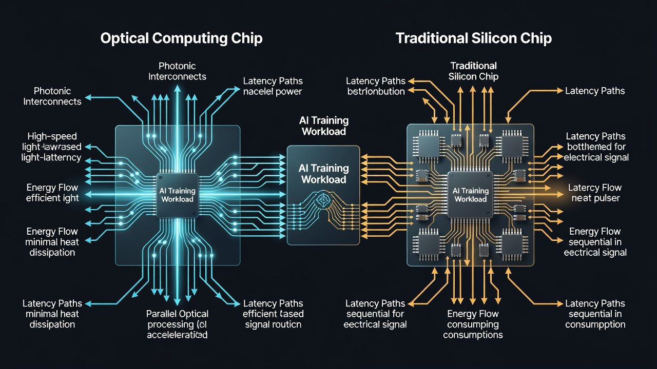
Traditional electronic silicon chips have powered data centers for decades, but their energy demands have grown unsustainable amid exploding AI requirements. Optical alternatives address this by transmitting data via photons, which generate far less heat and enable higher bandwidth over distance without the resistive losses inherent in copper traces. This fundamental physics advantage allows data centers to handle larger model training runs while staying within existing power envelopes.
How Optical Computing Works
Optical computing chips leverage waveguides, modulators, and photodetectors fabricated on silicon photonics platforms. Data is encoded onto laser light at multiple wavelengths, enabling parallel processing that electronic chips achieve only through complex multiplexing. In practice, matrix multiplications central to neural networks occur in the optical domain with minimal conversion steps, reducing both energy per operation and end-to-end latency.
Engineers integrate these components using hybrid bonding techniques that combine III-V laser sources with CMOS-compatible photonics. The result is a processor that maintains coherence across racks while consuming a fraction of the power required for equivalent electronic signaling.
Energy Efficiency and Latency Comparison
Benchmarks from leading providers highlight stark differences. Optical chips demonstrate up to 10x better energy efficiency in matrix multiplication tasks central to AI models, with latency reductions of 30-50% in interconnect-heavy operations. Real-world tests in 2026 show electronic silicon chips consuming significantly more power per teraflop, while optical versions maintain performance under sustained loads with minimal cooling overhead.
Key metrics include lower bit-error rates in optical interconnects and reduced signal degradation, allowing tighter integration in rack-scale architectures. These advantages compound in large clusters where interconnect power dominates total consumption. Teams also note improved thermal stability, which extends hardware lifespan and reduces maintenance cycles.
Real Deployment Benchmarks from Leading Providers
Independent testing labs and cloud providers have published side-by-side results comparing optical accelerators against the latest electronic GPUs. In controlled environments, optical systems delivered consistent 4-8x improvements in tokens processed per kilowatt-hour during large language model pre-training. Latency for all-reduce operations dropped by nearly half when optical fabrics replaced traditional high-speed Ethernet links.
These benchmarks were gathered across multiple hardware generations and validated using standardized workloads from MLPerf. Providers emphasize that gains scale with cluster size, making optical solutions particularly attractive for frontier model development.
Case Studies from Cloud Operators
Major providers have begun integrating optical computing chips into production environments. One hyperscaler reported deploying photonic accelerators across 15% of its AI training fleet by mid-2026, achieving substantial energy reductions without sacrificing throughput. Another operator integrated the technology into inference pipelines, noting faster response times for real-time applications such as recommendation engines and autonomous systems.
A third cloud provider focused on sustainability metrics, documenting a 40% drop in power usage effectiveness after retrofitting select availability zones. These deployments underscore practical benefits: operators cite easier scaling of GPU-like workloads and compatibility with existing orchestration tools after firmware updates. Lessons learned include the importance of early collaboration with foundry partners to secure supply.
Practical Integration Steps for IT Teams
IT teams considering adoption should follow a structured approach:
- Assess current workloads to identify AI training or inference tasks with high interconnect demands, using profiling tools to quantify power and latency bottlenecks.
- Evaluate hardware compatibility through vendor-provided SDKs and simulation tools that model photonic signal integrity within existing rack layouts.
- Pilot small clusters in isolated environments to measure power draw and latency, comparing results against baseline electronic silicon performance over at least four weeks.
- Update network fabrics to support optical transceivers and retrain staff on photonic diagnostics, including monitoring for laser degradation and alignment drift.
- Scale gradually while monitoring thermal profiles and total cost of ownership, incorporating feedback loops from operations teams to refine deployment playbooks.
These steps minimize disruption while maximizing early returns on efficiency. Many teams also establish cross-functional working groups that include facilities, networking, and machine learning engineers.
Manufacturing Challenges and Cost Projections
Scaling optical chip production involves hurdles such as precise lithography for photonic waveguides and integration with CMOS processes. Yield rates have improved steadily, yet challenges remain in aligning laser sources and detectors at scale. Industry roadmaps point to broader availability by late 2026 as foundries refine hybrid integration techniques.
Qualitative trends show declining per-unit costs as volumes rise, driven by demand from AI infrastructure builders. Continued investment in automated testing and packaging will further accelerate adoption.
Learn more about energy efficiency initiatives at the U.S. Department of Energy. Additional guidance on emerging hardware standards is available from NIST.
Performance Metrics in AI Training Workloads
In AI-specific benchmarks, optical chips excel at parallel linear algebra operations, delivering higher tokens-per-watt in large language model training. Teams report completing epochs faster with lower electricity draw, enabling more experiments within the same power budget. Latency gains prove especially valuable in distributed training across thousands of nodes where synchronization overhead previously limited scaling efficiency.
Real examples include training runs on recommendation models that finished 35% sooner while using 60% less energy for interconnect traffic. These metrics position optical computing as a key enabler for next-generation foundation models.
Environmental Impact and Sustainability Benefits
Beyond direct energy savings, optical chips reduce the carbon footprint of data centers by lowering cooling requirements and extending equipment life. Operators aligning with global sustainability targets find photonic solutions helpful in meeting Scope 3 emissions goals. IEEE resources on sustainable computing provide further context for long-term planning.
Future Scalability and Compatibility Considerations
Looking ahead, optical computing is expected to complement rather than replace electronic silicon in hybrid architectures. Compatibility layers and standardized interfaces are evolving to support mixed deployments. Scalability hinges on continued advances in packaging and software ecosystems that abstract photonic specifics from developers.
FAQ
Are optical chips compatible with existing data center infrastructure?
Many designs include backward-compatible interfaces, though optical transceivers often require updates to cabling and switches for full benefit. Most vendors supply migration guides and reference architectures.
How does scalability look for future AI models?
Early deployments indicate strong scaling potential, with performance advantages growing as model sizes increase and interconnect traffic intensifies. Hybrid designs allow gradual transition without forklift upgrades.
What manufacturing timelines are realistic?
Volume production is ramping through 2026, with broader commercial availability anticipated by year-end depending on foundry capacity and yield improvements.
Will software need major rewrites?
Most frameworks already support accelerator abstraction layers, so code changes are typically limited to configuration and optimization flags rather than full rewrites.
Optical computing chips represent a transformative step toward sustainable, high-performance data centers in the AI era. Organizations that begin evaluation now will be best positioned to capitalize on the efficiency gains emerging throughout 2026 and beyond.
No comments yet. Be the first!