 NeoBit Daily

Introduction to Optical Computing Chips and GPUs in 2026 AI Landscapes
As artificial intelligence workloads continue to scale dramatically in 2026, enterprises are evaluating next-generation hardware solutions to meet growing computational demands. Optical computing chips, which leverage photons instead of electrons for data processing, are emerging as strong contenders against traditional GPUs. This comparison explores their deployments in depth, focusing on performance metrics, energy savings, real-world enterprise adoption, and integration realities in data centers and edge environments. Industry leaders seek solutions that balance raw speed with sustainability, and optical technologies promise breakthroughs in both areas while addressing the limitations of electron-based systems that have dominated for decades.
Understanding the Core Technologies
GPUs have powered AI training and inference for years through massive parallel processing architectures optimized for matrix operations. Optical computing chips, however, transmit data via light waves through waveguides and modulators, enabling potentially lower latency and reduced heat generation. In 2026, hybrid systems combining both technologies are becoming common in cloud infrastructures, allowing organizations to route specific tasks to the most suitable hardware. Photonic chips excel at linear algebra computations central to deep learning, while GPUs provide flexible programmability for diverse model architectures. This synergy creates opportunities for more efficient pipelines in large-scale deployments.
Performance Gains and Benchmarks
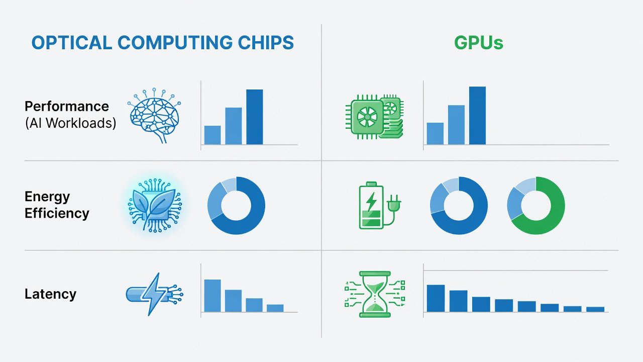
Early 2026 deployments show optical chips achieving significant throughput improvements in matrix multiplications critical for neural networks. Side-by-side benchmarks reveal optical solutions excelling in specific inference tasks while GPUs maintain advantages in versatile training scenarios involving frequent updates. Practical testing in controlled environments demonstrates optical chips handling high-volume data streams with minimal signal degradation over distance. Organizations report smoother scaling when workloads are partitioned intelligently between the two hardware types.
- Optical chips demonstrate up to 5x faster data movement in photonic interconnects compared to electrical pathways.
- GPUs offer mature software ecosystems like CUDA for rapid prototyping and debugging.
- Combined systems deliver balanced workloads across training and inference stages in AI pipelines.
- Latency-sensitive applications benefit from optical speed in real-time decision making.
Energy Efficiency Metrics
Energy consumption remains a key concern for large-scale AI operations running continuously. Optical computing reduces power draw by minimizing electrical resistance and associated heat, leading to substantial efficiency gains in sustained operations. Data center operators note that photonic approaches allow higher compute density without proportional increases in cooling infrastructure. This efficiency translates into operational advantages for hyperscale environments where power availability often constrains expansion. Qualitative improvements in sustainability metrics help companies meet environmental goals while maintaining performance targets.
Latency Reductions in Data Centers
Photon-based transmission slashes communication delays between processors and memory subsystems. This is particularly beneficial for real-time AI applications where milliseconds matter, such as autonomous systems and financial modeling. Reduced latency enables tighter feedback loops in distributed training clusters, accelerating overall model convergence times. Enterprises deploying these technologies observe measurable improvements in user-facing AI services that require instantaneous responses.
Enterprise Adoption and Cost Savings Examples
Major cloud providers are piloting optical integrations, citing improved scalability for expanding AI services. While exact figures vary by implementation, qualitative savings arise from lower cooling requirements and higher density deployments that maximize existing floor space. NVIDIA continues evolving GPU architectures alongside these shifts, ensuring compatibility pathways for customers exploring hybrid solutions. Adoption is accelerating as proof-of-concept projects demonstrate reliable returns through optimized resource utilization.
Integration Challenges with Existing Infrastructure
Transitioning to optical chips involves overcoming compatibility hurdles with legacy silicon-based systems still prevalent in most facilities. Key challenges include developing new photonic interfaces that align with current networking standards and retraining engineering teams on light-based architectures. Supply chain considerations also play a role, as specialized materials for photonic components require new vendor relationships. Successful integrations typically begin with modular additions rather than full replacements, allowing gradual migration without disrupting ongoing operations. Organizations must also address software stack adaptations to fully exploit optical acceleration capabilities.
Case Studies from Automotive and Robotics Sectors
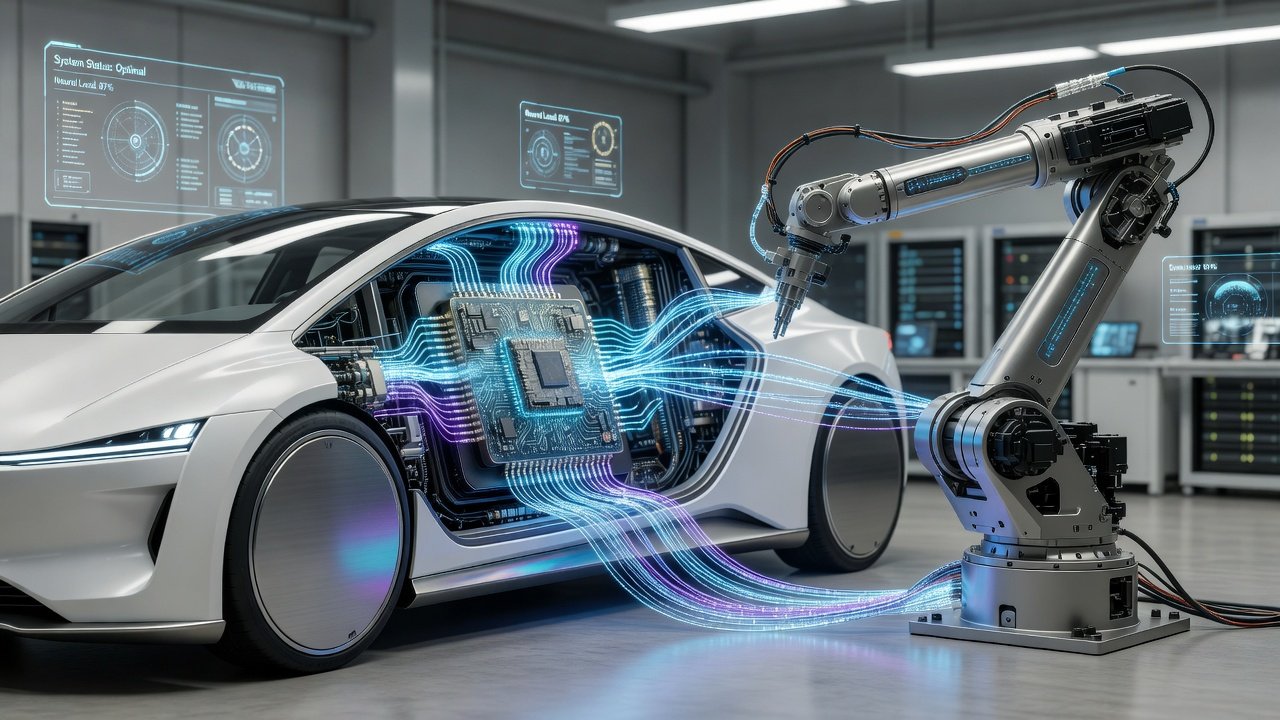
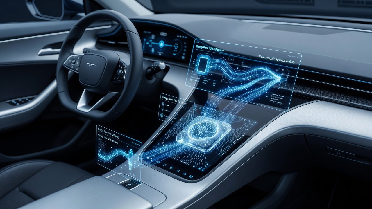
In automotive applications, optical chips enable faster sensor data processing for self-driving vehicles, where rapid interpretation of lidar and camera inputs is essential for safety. Robotics firms leverage them for precise, low-power edge AI, improving battery life in mobile units operating in warehouses or manufacturing floors. These sectors highlight the practical value of reduced energy needs combined with high-speed computation. IBM and Intel have contributed foundational research supporting these industry applications, with ongoing collaborations yielding deployable prototypes. Additional examples from healthcare imaging and financial services further illustrate broad applicability across domains requiring both speed and efficiency.
Practical Implementation Steps and FAQs
Steps for Adoption
- Assess current AI workload profiles for photonic suitability by analyzing compute patterns and data movement requirements.
- Pilot hybrid optical-GPU setups in controlled environments to measure real-world gains against baselines.
- Evaluate software frameworks supporting optical accelerators and plan necessary code optimizations.
- Monitor performance metrics continuously and scale gradually based on validated results.
- Engage with hardware vendors early to secure supply and customization support for specific use cases.
Frequently Asked Questions
How do optical chips compare in versatility to GPUs? They shine in specialized linear algebra tasks but require GPU support for broader applications involving branching logic or irregular data structures.
What are the main barriers to widespread use? Manufacturing maturity, ecosystem development, and initial integration complexity remain ongoing focuses for the industry in 2026.
Are there proven real-world deployments? Yes, select hyperscalers and automotive leaders have announced successful trials in 2026 demonstrating reliability at scale.
How should teams prepare for the transition? Focus on upskilling in photonics concepts and testing modular additions to existing clusters before full commitment.
Future Scalability and Conclusion
Optical computing chips represent a promising evolution for AI infrastructure as demands grow exponentially. As research advances through 2026 and beyond, their role alongside GPUs will likely expand, driving more efficient and capable systems across industries. IEEE resources provide further reading on photonic computing standards and emerging best practices. Enterprises evaluating these technologies should prioritize hybrid strategies for optimal results, ensuring they remain competitive while navigating the shift toward light-based processing. The combination of performance, efficiency, and practical case evidence positions optical solutions as a key element in the next phase of AI hardware evolution.
No comments yet. Be the first!