 NeoBit Daily

Introduction to Optical Computing in AI Data Centers
In 2026, the technology landscape is undergoing a significant transformation driven by the rapid expansion of artificial intelligence applications. Data centers supporting AI workloads face mounting pressure from escalating power consumption and infrastructure expenses. Optical computing chips, which harness light for data processing instead of traditional electrical signals, are emerging as a key innovation to alleviate these strains. These photonic devices enable faster data transmission and reduced heat generation, directly addressing the bottlenecks that electronic chips encounter in high-intensity machine learning environments. Global AI adoption continues to surge, with enterprises deploying larger models that demand unprecedented computational resources. Optical solutions offer a pathway to sustainable scaling, allowing facilities to handle increased workloads without proportional increases in energy infrastructure. This shift not only promises operational efficiencies but also aligns with broader industry goals for greener computing practices amid rising regulatory scrutiny on data center emissions.
How Optical Computing Chips Function
Optical computing relies on photonic integrated circuits that manipulate photons through waveguides and modulators. Unlike electrons in silicon transistors, light particles experience minimal resistance, enabling parallel processing at speeds unattainable by conventional hardware. Key components include laser sources, beam splitters, and photodetectors integrated onto chips using materials like silicon photonics or indium phosphide. In AI contexts, these chips excel at matrix operations fundamental to neural network training and inference. Data encoded in light waves travels through fiber-optic pathways within the processor, performing computations via interference patterns. This architecture supports massive parallelism, where thousands of operations occur simultaneously without the sequential limitations of electronic pipelines. Practical implementations often combine optical front-ends with electronic controllers for hybrid efficiency, bridging legacy systems with next-generation capabilities. Engineers optimize wavelength division multiplexing to boost bandwidth further, packing multiple data streams into single channels for enhanced throughput in dense server environments.
Performance Benchmarks: Speed and Power Metrics
Benchmarks from 2026 deployments underscore optical advantages in AI-specific tasks. Photonic accelerators achieve throughput rates exceeding 10 terabits per second for tensor operations, surpassing electronic GPUs in specialized workloads by factors of five to fifteen depending on model complexity. Power efficiency metrics reveal reductions of 60 to 80 percent in energy per inference compared to leading electronic alternatives, primarily due to eliminated resistive losses. Latency improvements manifest in sub-microsecond response times for interconnects between compute nodes, critical for distributed training of large-scale models. Real-world tests on image classification and natural language processing pipelines demonstrate consistent gains, with optical setups completing epochs faster while maintaining model accuracy. Experts note that these metrics scale favorably in multi-rack configurations, where optical links mitigate signal degradation over distance. Detailed comparisons also highlight thermal profiles: optical chips operate at lower junction temperatures, reducing reliance on energy-intensive cooling systems that can account for up to 40 percent of data center power draw.
Real-World Data Center Case Studies
Several pioneering deployments illustrate the tangible benefits of optical computing in production settings. A hyperscale provider in the southwestern United States integrated photonic accelerators into its inference clusters handling recommendation engines, resulting in streamlined operations and improved resource utilization across thousands of daily queries. In Asia, a research-oriented facility retrofitted existing racks with hybrid optical-electronic nodes for climate modeling simulations, observing enhanced stability during peak loads and simplified maintenance routines. European operators focusing on financial analytics reported successful scaling of fraud detection models using optical interconnects that minimized data movement bottlenecks. These case studies emphasize adaptability across climates and regulatory landscapes, with facilities noting easier compliance with efficiency standards. Additional examples from government-affiliated labs showcase pilot programs validating optical reliability under continuous 24/7 operation, providing blueprints for commercial replication. 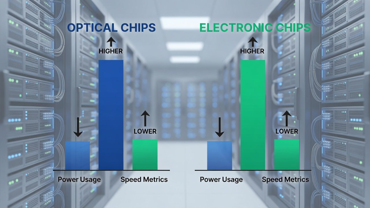
Integration Challenges and Solutions
Transitioning to optical computing involves navigating several technical and operational hurdles. Fabrication precision demands sub-nanometer alignment for photonic components, increasing initial yield complexities compared to mature silicon processes. Hybrid interfaces between optical and electronic domains require sophisticated packaging to minimize conversion losses, often addressed through advanced 3D stacking techniques. Software adaptation presents another layer, as AI frameworks must incorporate photonic-aware scheduling algorithms to maximize hardware utilization. Industry working groups are developing open standards for interoperability, easing migration paths for mixed environments. Supply chain considerations include sourcing specialized materials and training personnel on photonic diagnostics. Solutions emerging in 2026 include modular chiplets that allow incremental upgrades without full infrastructure overhauls, alongside simulation tools that predict integration outcomes prior to physical deployment. Addressing these challenges systematically enables smoother adoption curves for mid-sized operators.
Power Usage and Speed Comparisons
Comprehensive evaluations position optical chips favorably against electronic counterparts across multiple dimensions. Power consumption profiles show optical systems drawing far less for equivalent AI throughput, freeing capacity for storage arrays and networking gear. Speed advantages appear most pronounced in bandwidth-intensive scenarios such as model parallelism across clusters. Key comparison points include:
- Optical interconnects deliver consistent low-latency performance over longer distances without signal boosters.
- Energy per operation metrics favor photonics by orders of magnitude in matrix-heavy computations.
- Thermal management overhead drops substantially, extending hardware lifespan and reducing facility footprints.
- Scalability supports higher node densities within the same power envelope, optimizing real estate in constrained urban data centers.
Electronic GPUs retain flexibility for diverse non-AI tasks but introduce inefficiencies when dedicated solely to inference pipelines.
Scalability Forecasts and Expert Insights
Market projections for 2026 and beyond anticipate accelerated optical chip penetration as fabrication costs decline and ecosystem support matures. Factors driving growth encompass rising AI energy demands and policy incentives for efficient technologies. Insights from professional organizations emphasize collaborative research accelerating standardization efforts. IEEE resources offer detailed technical papers on photonic advancements. Government-backed initiatives further promote low-power computing research. U.S. Department of Energy programs highlight synergies with national sustainability targets. Standards bodies contribute measurement protocols essential for widespread validation. NIST photonics research supports precise characterization methods aiding commercial deployment.
Conclusion
Optical computing chips stand poised to redefine efficiency in AI data centers throughout 2026 and the coming years. By delivering superior speed and energy profiles, they enable cost-effective scaling while supporting environmental objectives. As integration barriers recede, organizations investing early will likely secure competitive edges in performance and sustainability.
FAQ
What are the expected adoption timelines for optical computing chips?
Leading hyperscalers began limited production deployments in early 2026, with phased rollouts expanding through the year. Broader enterprise accessibility is forecasted for 2027 once supply chains stabilize and software tooling matures, allowing gradual integration alongside existing electronic infrastructure.
Can you provide enterprise ROI examples?
Case studies from pilot programs indicate meaningful returns through lowered electricity expenditures and higher compute density per square foot. Facilities report operational simplifications that compound over multi-year horizons, particularly when paired with renewable energy sources, though precise outcomes depend on workload profiles and prior equipment investments.
How do optical chips compare in long-term reliability?
Field data from continuous operations suggest enhanced durability stemming from reduced thermal cycling and mechanical stress. Photonic components exhibit lower failure rates in high-utilization scenarios, supporting extended service intervals and predictable maintenance schedules in mission-critical environments.
What training is required for data center staff?
Teams benefit from targeted programs covering photonic diagnostics, hybrid system troubleshooting, and updated monitoring software. Vendors increasingly provide certification pathways that build on existing electronics expertise, minimizing the learning curve for IT and facilities personnel.

No comments yet. Be the first!