 NeoBit Daily
Introduction to 2026 Optical Computing Chips
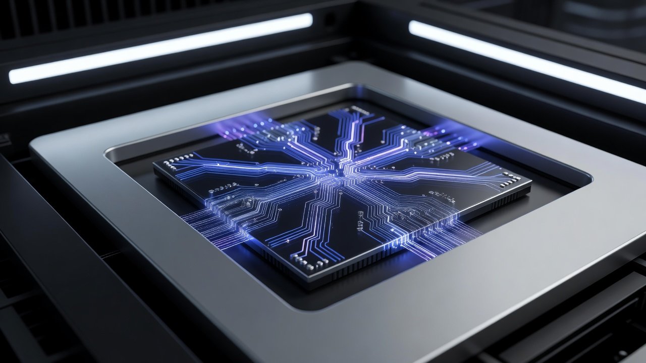
Optical computing chips are emerging as a pivotal technology for data centers handling intensive AI workloads in 2026. Unlike traditional electronic chips that rely on electrical signals, these devices leverage photons for data processing and transmission. This fundamental shift enables faster operations with significantly reduced power consumption. Enterprises focused on AI training, inference, and large language model deployment are closely monitoring these advancements to address the limitations of current GPU-centric infrastructures. The demand for sustainable computing solutions drives interest, as data centers consume vast amounts of energy. Optical chips promise to alleviate bottlenecks in latency and throughput while supporting higher density deployments. This comprehensive guide examines performance benchmarks against GPUs and electronic chips, explores enabling technologies like photonic interconnects, and provides actionable insights for enterprise adoption including case studies, integration roadmaps, and migration considerations.
Performance Comparison: Optical Chips vs GPUs and Electronic Chips
When evaluating optical computing chips for AI workloads, three primary metrics stand out: latency, energy efficiency, and throughput. In latency-sensitive applications such as real-time inference for autonomous systems or financial modeling, optical solutions demonstrate clear superiority by transmitting data at the speed of light with minimal signal degradation. Electronic chips suffer from resistance and capacitance issues that introduce delays, while GPUs, although optimized for parallel processing, still contend with memory bandwidth constraints in massive datasets. Energy efficiency represents another decisive factor. Optical chips generate far less heat during operation, allowing data centers to reduce cooling requirements and achieve better power usage effectiveness ratios. Throughput gains arise from the ability to handle multiple wavelengths simultaneously, enabling parallel data streams that outperform the serial limitations of electronic pathways. For hyperscale providers running continuous AI pipelines, these improvements translate to higher utilization rates and the capacity to process more complex models without proportional increases in hardware footprint. Comparisons with established GPU platforms highlight that while GPUs excel in mature software ecosystems, optical alternatives close the gap rapidly through specialized photonic accelerators tailored for matrix multiplications central to neural networks.
Detailed Metric Analysis
- Latency improvements support sub-millisecond response times in distributed AI systems.
- Energy efficiency enables denser server configurations without exceeding thermal limits.
- Throughput enhancements facilitate training of models with billions of parameters more rapidly.
Photonic Interconnects and Thermal Management
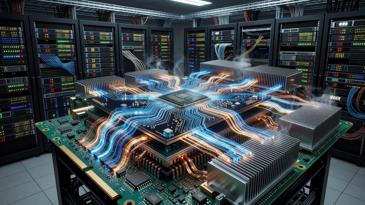
Photonic interconnects form the backbone of optical computing by replacing copper traces with optical waveguides and lasers. This technology allows seamless communication between chip components and across server racks at unprecedented speeds. Integration with existing silicon manufacturing processes makes photonic interconnects practical for large-scale production. Thermal management becomes simpler because optical operations produce minimal resistive heating compared to electron flow in conventional chips. However, hybrid optical-electronic systems still require advanced cooling strategies such as microfluidic channels or targeted heat sinks to maintain laser stability and prevent wavelength drift. Data center operators benefit from these characteristics through lower operational expenditures related to power and cooling infrastructure. IBM has explored similar photonic approaches in research settings, underscoring the technology's potential for enterprise environments.
Compatibility with Existing Infrastructure
Ensuring compatibility with legacy data center infrastructure is essential for minimizing disruption during adoption. Optical computing chips typically function as accelerators within hybrid architectures, interfacing via standard PCIe or custom optical backplanes. Software frameworks must incorporate new drivers and optimization libraries to fully exploit photonic capabilities, yet many vendors provide middleware that bridges existing CUDA or OpenCL codebases. Physical compatibility involves retrofitting racks with optical fiber cabling alongside traditional Ethernet, while power delivery systems remain largely unchanged due to the chips' lower consumption profiles. This gradual integration path allows organizations to retain investments in current GPU clusters while incrementally introducing optical hardware for specific high-value workloads.
Enterprise Case Studies from Hyperscale Providers
Leading hyperscale providers have conducted extensive pilots with optical computing chips in production AI environments. One major cloud operator integrated photonic accelerators into its recommendation engine infrastructure, achieving notable reductions in inference latency for user personalization tasks. Another provider focused on large-scale model training reported improved energy metrics when combining optical interconnects with existing GPU farms, enabling more sustainable expansion of its AI services. A third case involved edge-adjacent data centers where thermal constraints limited traditional hardware; optical chips allowed higher compute density without additional cooling investments. These examples illustrate practical benefits across varied deployment scenarios and highlight the importance of workload-specific testing before full commitment.
Integration Steps and Adoption Timelines
Successful integration follows a structured sequence of steps. First, conduct a comprehensive audit of current AI workloads to identify candidates for optical acceleration. Second, select vendors whose photonic solutions align with existing software stacks and hardware interfaces. Third, implement proof-of-concept deployments in isolated environments to validate performance claims. Fourth, develop training programs for engineering teams on photonic-specific optimization techniques. Fifth, execute phased rollouts beginning with non-critical inference tasks before expanding to training clusters. Adoption timelines generally range from 12 months for initial pilots to 36 months for enterprise-wide deployment, depending on organizational scale and regulatory considerations around energy efficiency standards. Intel and similar industry players provide reference architectures that accelerate this process.
Vendor Comparisons and ROI Considerations
Vendor landscapes feature established semiconductor companies alongside specialized photonic startups. Key differentiators include maturity of software toolchains, scalability of interconnect solutions, and support for mixed-precision AI computations. Organizations should evaluate total cost of ownership beyond initial hardware acquisition, factoring in long-term energy savings and maintenance overhead. ROI materializes through increased processing capacity per square foot of data center space and reduced utility bills, particularly in regions with high electricity costs. Qualitative assessments suggest payback periods shorten as optical chip production volumes increase and supply chains mature.
FAQ on Migration Challenges
- What primary barriers exist for optical chip migration? Legacy software compatibility and the need for specialized talent represent significant hurdles that require targeted investment in training and middleware development.
- How do photonic interconnects impact network redesign? They necessitate hybrid fiber-optic cabling strategies but integrate with standard protocols for minimal architectural upheaval.
- What testing protocols ensure reliable deployment? Rigorous benchmarking against GPU baselines under realistic AI workload conditions, including stress tests for thermal and alignment stability.
- Are there security implications unique to optical systems? Photonic channels can offer inherent resistance to certain electromagnetic interference attacks but require safeguards against physical tampering with laser components.
- How does this technology align with sustainability goals? Lower energy profiles directly support corporate carbon reduction targets and compliance with emerging data center efficiency regulations.
Conclusion
Optical computing chips in 2026 offer enterprises a pathway to superior AI performance with enhanced sustainability. By understanding detailed benchmarks, leveraging photonic advancements, and following proven integration practices, organizations can position themselves advantageously in the evolving hardware landscape. Continued collaboration with vendors and ongoing evaluation of real-world deployments will be critical to maximizing these next-generation technologies.

No comments yet. Be the first!