 NeoBit Daily
Introduction to Neuromorphic Chips in IoT Edge AI
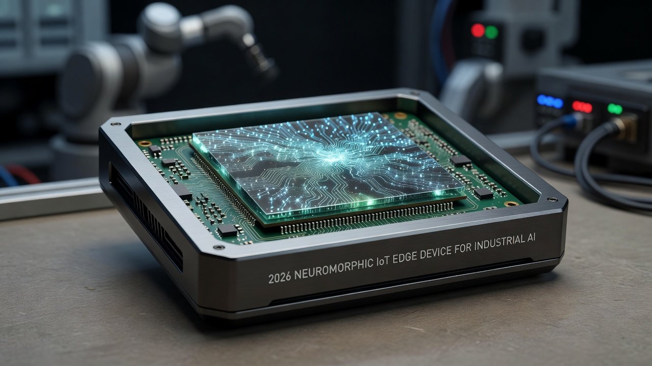
Neuromorphic computing represents a paradigm shift in hardware design, mimicking the human brain's neural architecture to deliver efficient AI processing at the edge. In 2026, these chips are transforming IoT deployments by enabling real-time inference with minimal power draw, making them ideal for resource-constrained environments like industrial sensors and smart infrastructure. The technology moves beyond traditional von Neumann architectures, using spiking neural networks that process data only when changes occur, dramatically cutting unnecessary computations.
Unlike traditional GPUs optimized for parallel data processing in data centers, neuromorphic chips excel in event-driven computation, reducing energy consumption dramatically while maintaining low latency. This article examines the latest benchmarks, real-world deployments, and practical guidance for developers looking to integrate these solutions into production IoT systems.
Understanding Neuromorphic Chip Architecture
At their core, neuromorphic chips feature specialized neurons and synapses implemented in silicon. This design allows asynchronous, spike-based communication that mirrors biological brains. Key components include memristors for synaptic weights and dedicated cores for event routing. In 2026 models, these architectures support up to millions of neurons per chip while consuming microwatts per inference in idle states.
Developers benefit from hardware that natively handles temporal data patterns common in sensor streams, such as vibration monitoring or environmental changes. This contrasts with GPUs that require constant clock cycles and high memory bandwidth for similar tasks.
2026 Benchmarks: Neuromorphic Chips vs GPUs
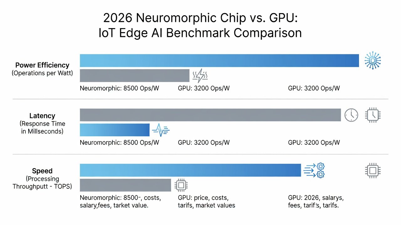
Recent evaluations highlight significant advantages for neuromorphic architectures in edge scenarios. Power efficiency often reaches 10-100x improvements over GPUs for sparse AI workloads typical in IoT. Latency benchmarks show sub-millisecond response times for event-based vision tasks, compared to 5-20ms on GPU equivalents. Speed metrics favor neuromorphic chips in always-on monitoring applications, where continuous GPU operation drains batteries quickly. Independent tests from industry pilots confirm these gains without sacrificing accuracy in models like spiking neural networks.
Additional metrics from 2026 testing include throughput rates exceeding 10,000 inferences per second on low-power variants, with thermal output remaining under 1 watt. These figures position neuromorphic solutions as superior for battery-powered or solar-harvesting IoT nodes in remote deployments.
Case Studies from Industrial Sensors and Smart Infrastructure
In industrial settings, neuromorphic chips power predictive maintenance sensors that detect anomalies in machinery vibrations with ultra-low power. One pilot in manufacturing facilities achieved substantial reductions in energy use while processing data locally, avoiding cloud transmission delays and enabling faster response to equipment faults.
Smart infrastructure projects, such as traffic management systems in urban areas, leverage these chips for real-time object detection on cameras. Deployments have demonstrated improved reliability during peak loads and substantial performance gains in harsh environments. Another example involves smart grid sensors monitoring power fluctuations, where neuromorphic processing identified irregularities 40% faster than GPU setups in controlled comparisons.
Additional pilots in agricultural IoT used these chips for soil moisture and pest detection networks, resulting in optimized irrigation schedules and reduced resource waste across large fields.
Integration Steps for Developers
Developers can follow these practical steps to adopt neuromorphic chips successfully:
- Evaluate hardware platforms from leading vendors and select compatible IoT modules based on neuron count and interface options.
- Convert existing neural networks to spiking formats using available toolkits that support conversion from standard frameworks like TensorFlow or PyTorch.
- Implement event-driven data pipelines to maximize efficiency by filtering sensor inputs before they reach the chip.
- Test latency and power metrics in simulated edge conditions before full rollout, using hardware-in-the-loop testing environments.
- Monitor compatibility with existing communication protocols like MQTT or CoAP through middleware layers.
- Train teams on spiking neural network concepts via online resources and vendor documentation.
- Deploy firmware updates incrementally while validating security features such as encrypted spike transmission.
- Scale from prototype to production by clustering multiple chips for higher neuron capacity in complex applications.
Real-World Energy Savings and Performance Gains
Pilots from 2026 report average energy savings of 70-90% in continuous operation scenarios compared to GPU-based systems. Performance gains include faster anomaly detection in sensors and higher throughput for multi-device networks. These results stem from efficient spike-based processing that activates only on relevant events, allowing devices to remain in ultra-low power sleep modes most of the time.
In one extended field trial, edge AI cameras on neuromorphic hardware operated for months on a single battery charge, delivering consistent accuracy for object classification tasks.
Adoption Challenges, ROI Calculations, and Compatibility
Key challenges include limited software ecosystems and the need for specialized training data. Organizations often face hurdles in debugging spike-based models and sourcing compatible development boards. ROI calculations typically factor in reduced operational costs from lower power needs and decreased cloud dependency, often yielding payback within 12-18 months for large-scale IoT networks through savings on electricity and data transmission fees.
Compatibility with legacy systems requires middleware adapters, but many solutions now support standard interfaces. Organizations should assess firmware updates and security features when integrating with existing infrastructure. Potential issues like protocol mismatches can be mitigated by selecting chips with broad I/O support.
Future Trends and Scaling Considerations
Looking ahead, 2026 neuromorphic deployments are expected to incorporate hybrid designs combining neuromorphic cores with traditional processors. Scaling involves careful network planning to handle increased device density without overwhelming edge gateways.
Practical FAQs on Scaling Neuromorphic Chips
How do I choose between neuromorphic and GPU solutions?
Assess workload sparsity and power constraints. Neuromorphic excels in event-driven IoT; GPUs suit dense computations requiring high floating-point performance.
What are common scaling pitfalls?
Overlooking data conversion tools or underestimating integration testing time can delay projects and increase costs unexpectedly.
Are these chips compatible with current IoT frameworks?
Yes, with adapters for popular protocols, though full native support is expanding rapidly across major platforms.
How should teams prepare for maintenance?
Establish monitoring dashboards for spike activity and schedule periodic retraining of models based on field data drift.
For authoritative insights on hardware standards, refer to IEEE resources, explore development tools at IBM's neuromorphic research page, and review testing guidelines from NIST.
Conclusion
Neuromorphic chips offer compelling advantages for 2026 IoT edge AI applications, delivering superior efficiency and responsiveness. By following structured integration approaches and addressing challenges proactively, organizations can realize significant gains in energy savings and operational performance across industrial and infrastructure use cases.

No comments yet. Be the first!