 NeoBit Daily

Introduction to 3D-Printed Electronics in 2026
The world of electronics prototyping is undergoing a seismic shift in 2026. Additive manufacturing techniques now allow engineers to print functional circuits, sensors, and even complete components directly, slashing development timelines from weeks to days. This evolution, highlighted across major 2026 tech news outlets, is particularly impactful in automotive and consumer device sectors where rapid iteration drives competitive advantage. Engineers are moving beyond traditional subtractive methods that require extensive chemical etching and mechanical drilling. Instead, layer-by-layer deposition of conductive and insulating materials creates complex geometries that were previously impossible or prohibitively expensive to manufacture. Real-world updates from industry conferences show that prototypes once requiring multiple vendor handoffs can now be completed in-house within a single shift.
Traditional PCB fabrication involves multiple steps including etching, drilling, and assembly. In contrast, 3D printing fuses conductive inks and dielectric materials in a single process. Real-world updates show leading labs achieving functional prototypes in under 24 hours, compared to the 5-10 days typical of conventional methods. This acceleration is not merely incremental; it fundamentally changes how teams approach design validation and risk mitigation in fast-moving markets.
Speed, Cost, and Material Performance Comparisons
Comparative analyses from industry reports reveal stark differences. 3D-printed electronics deliver prototypes up to 80% faster, primarily by eliminating mask creation and chemical processing. Material performance has advanced significantly; modern conductive polymers now match 90% of copper's conductivity while offering flexibility for curved surfaces. Engineers report improved thermal stability in printed traces, allowing operation in high-temperature environments such as engine compartments without additional heat sinks.
Cost-wise, the approach reduces material waste by 60-70% and lowers tooling expenses. Case studies from automotive labs demonstrate a single 3D-printed sensor array requiring fewer resources than traditional equivalents when factoring in labor and iteration cycles. Beyond direct savings, the technology enables concurrent engineering where mechanical and electrical teams iterate simultaneously on the same digital model.
Real-World Industry Case Studies
In the automotive sector, a major European manufacturer used 3D-printed electronics to prototype in-vehicle radar housings. The process integrated antennas directly into structural components, cutting development from three weeks to four days. Consumer device firms have applied similar techniques to wearable health monitors, printing flexible circuits that conform to the body while embedding biometric sensors in a single print run. These examples illustrate how the technology bridges the gap between concept and functional testing with minimal intermediate steps.
Leading research labs, including those affiliated with MIT, have published results on hybrid printing methods combining rigid and flexible substrates for IoT devices. Additional work at university facilities has focused on multi-material printing that incorporates both passive components and active semiconductors in one build, further compressing the validation timeline for connected products.
Scalability Challenges in Additive Electronics Manufacturing
Despite rapid progress, scalability remains a hurdle. High-volume production still faces limitations in print speed and consistency across large batches. Engineers must address issues like layer adhesion and thermal management in printed traces. Current solutions involve multi-nozzle systems and post-processing sintering, yet full factory-scale adoption requires further material science advances. Production teams often encounter variability in conductivity when scaling from laboratory printers to industrial models, necessitating rigorous quality control protocols at each stage.
Early adopters recommend starting with low-volume runs under 500 units to validate designs before scaling. Additional challenges include supply chain readiness for specialized inks and the need for standardized file formats that translate seamlessly between CAD software and printer firmware. Addressing these requires cross-functional collaboration between materials scientists, electrical engineers, and manufacturing specialists.
Integration with AI Design Tools
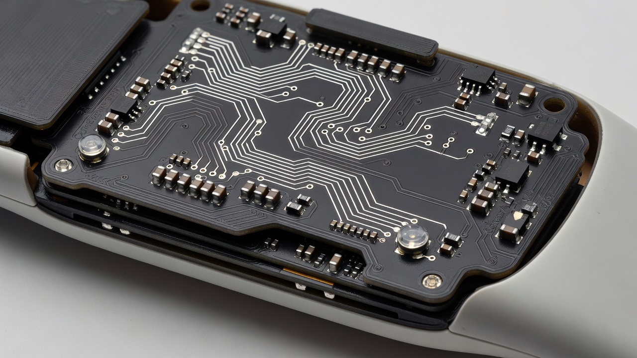
AI is accelerating the workflow dramatically. Machine learning algorithms optimize trace layouts for minimal resistance and maximal signal integrity, often generating designs in minutes that would take human engineers hours. Tools from major tech providers now simulate electromagnetic performance before printing begins, reducing failed prototypes by up to 40%. Generative design capabilities allow the system to propose unconventional routing that maximizes space utilization within constrained enclosures.
This synergy allows generative design where AI proposes novel 3D circuit geometries tailored to specific mechanical constraints. Integration with existing PLM systems further streamlines data flow, ensuring that printed prototypes carry full traceability from initial simulation through physical testing. Engineers benefit from automated error detection that flags potential short circuits or insufficient clearance before material is deposited.
Material Innovations and Environmental Considerations
Recent advancements have introduced bio-based conductive inks and recyclable dielectric substrates that align with sustainability goals. These materials maintain performance while reducing reliance on rare earth elements traditionally used in electronics. Environmental impact assessments indicate lower energy consumption during production compared to conventional PCB etching processes that involve hazardous chemicals.
Teams evaluating these options should review compatibility with existing recycling streams and conduct lifecycle analyses specific to their product categories. Such considerations are becoming increasingly important as regulatory frameworks tighten around electronic waste.
Early Adoption Examples and Practical Steps for Engineers
Companies in Silicon Valley and Stuttgart have integrated 3D electronics into their standard pipelines. For implementation, engineers should follow a structured approach:
- Evaluate compatible printers supporting multi-material extrusion with silver nanoparticle inks and verify vendor support for ongoing maintenance and material updates.
- Partner with material suppliers offering certified conductive filaments that meet industry standards for conductivity and durability.
- Run pilot projects focusing on non-critical components first to build internal expertise and identify workflow bottlenecks.
- Train teams on design software that exports directly to printer G-code while incorporating simulation modules for electrical performance.
- Establish metrics for success such as time-to-first-functional-prototype and iteration count per design cycle.
Regulatory hurdles include compliance with EMC standards and material safety certifications. Bodies like the FDA are developing guidelines for printed medical electronics, emphasizing traceability and biocompatibility testing. Additional oversight from organizations such as IEEE addresses electromagnetic compatibility for printed assemblies in consumer and automotive applications.
Conclusion
3D-printed electronics represent a pivotal advancement in 2026 prototyping. By combining speed, design freedom, and AI assistance, the technology is reshaping how industries innovate. Engineers ready to adopt should focus on targeted pilots while monitoring evolving standards and material developments to ensure long-term success.
FAQ
What are the first steps for an engineer to implement 3D-printed electronics?
Begin by auditing current prototyping bottlenecks, then select a desktop or industrial printer suited to your scale. Test basic conductive traces before advancing to integrated components. Document each iteration to build a knowledge base for future projects.
What regulatory hurdles exist for 3D-printed electronics?
Key challenges involve meeting electromagnetic compatibility (EMC) requirements and obtaining material certifications. Early engagement with standards organizations helps navigate these. Documentation of print parameters and material batches supports compliance audits.
How does 3D printing compare in cost to traditional methods as of 2026-09-04?
While exact figures vary, qualitative analyses show reduced waste and tooling costs make it advantageous for prototypes, with full production still requiring hybrid approaches in many cases. Organizations should perform internal cost modeling based on their specific volume and complexity.
What training is recommended for teams adopting this technology?
Focus on CAD-to-print workflows, material handling safety, and post-print testing procedures. Many suppliers offer certification programs that cover both hardware operation and design best practices.


No comments yet. Be the first!