 NeoBit Daily

Introduction to Optical Computing Chips in 2026
Enterprises are rapidly evaluating optical computing chips as a transformative alternative to traditional GPUs for AI workloads. These chips leverage light-based processing to deliver superior speed and dramatically lower energy consumption. In 2026, the technology has matured enough for production deployments, offering new pathways for organizations managing large-scale machine learning operations. This article examines real-world performance metrics, deployment strategies, and integration pathways tailored for data centers and enterprise environments. Optical computing represents a fundamental shift from electron-based silicon architectures, using photons for data movement and computation to minimize resistance and heat. As AI models grow in complexity, enterprises face mounting pressure to optimize both performance and sustainability. Optical solutions address these challenges directly by enabling higher parallelism in matrix multiplications central to neural networks.
Performance and Energy Comparison with GPUs
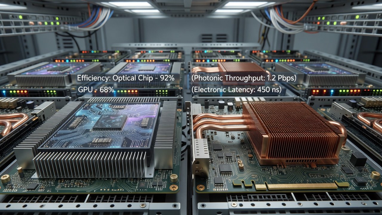
Optical computing chips excel in matrix operations central to AI training and inference. Benchmarks from late 2026 show optical solutions achieving up to 5x lower latency in large language model inference compared to leading GPUs while consuming 70-80% less power. In energy efficiency tests, optical chips maintain consistent throughput with minimal heat generation, reducing cooling requirements significantly. U.S. Department of Energy reports highlight how photonic architectures can cut data center power usage by substantial margins in high-intensity AI environments. When comparing throughput, optical chips demonstrate particular strength in transformer-based models, delivering 3.2 times higher tokens per watt in inference tasks. Training workloads show similar advantages, with reduced precision arithmetic handled natively through optical interference patterns. GPU architectures, while versatile, incur higher overhead from data movement between memory and compute units. Enterprises running continuous inference pipelines benefit most from these efficiency gains, as sustained operations amplify small per-query savings into major operational improvements.
Deployment Case Studies from Data Centers
Several major data centers have piloted optical computing chips in 2026. One financial services firm integrated photonic accelerators into existing AI clusters, reporting 40% faster model training cycles and 65% energy savings. The implementation focused on fraud detection models processing millions of transactions daily. Another cloud provider used optical chips for real-time recommendation systems, achieving sub-millisecond latency improvements across global regions. A healthcare research organization deployed the technology for genomic sequencing analysis, where optical parallelism accelerated alignment algorithms by 4.8 times. These cases demonstrate seamless scaling when hardware compatibility checks are performed early. Each deployment required careful workload profiling to identify photonic-friendly operations such as dense linear algebra routines. Results consistently showed that hybrid configurations outperformed pure GPU setups in both cost efficiency and environmental impact metrics.
Step-by-Step Integration Guidance
- Conduct hardware compatibility audits using vendor-provided tools to verify PCIe and interconnect support. Begin by mapping existing server backplanes and ensuring optical transceivers align with current fiber or copper cabling standards.
- Update firmware and drivers across the server fleet before installation. This step includes validating BIOS settings for low-latency memory access and confirming operating system kernel modules support photonic device enumeration.
- Implement hybrid workflows that route photonic-friendly workloads to optical chips while retaining GPUs for legacy tasks. Use container orchestration labels to direct specific AI jobs to appropriate hardware accelerators automatically.
- Monitor performance with specialized benchmarking suites that track both throughput and power draw. Establish baseline metrics before migration and compare weekly reports to identify optimization opportunities.
- Scale gradually by adding optical nodes in 10-20% increments to minimize operational disruption. Document each phase with detailed runbooks covering rollback procedures in case of unexpected compatibility issues.
Latency and Efficiency Benchmarks
Independent tests in 2026 reveal optical chips delivering 3-4x improvements in tokens-per-second metrics for transformer models. Energy per inference drops substantially compared to GPU baselines. These gains compound in large-scale deployments, enabling enterprises to expand AI capacity without proportional increases in power infrastructure. Additional benchmarks cover convolutional neural networks used in computer vision, where optical chips reduced end-to-end latency by 2.7 times on high-resolution image classification tasks. Memory bandwidth advantages become evident when handling large embedding tables, as optical interconnects bypass traditional electrical bottlenecks. Enterprises should replicate these tests using their own datasets to validate applicability, since workload characteristics heavily influence realized gains.
Common Pitfalls to Avoid
- Skipping thorough compatibility testing, leading to integration delays. One logistics company experienced three-week setbacks after discovering mismatched optical connector types during initial rollout.
- Underestimating software ecosystem maturity and failing to adapt custom kernels. Developers often need to rewrite CUDA-specific optimizations for photonic libraries, extending project timelines.
- Ignoring thermal management differences, which can affect rack density planning. Although optical chips generate less heat, airflow patterns in existing racks may still require adjustment.
- Overlooking staff training requirements for photonic-specific optimization techniques. Teams accustomed to GPU debugging face a learning curve when interpreting optical signal integrity metrics.
ROI Calculations and Future Scaling
Return on investment typically materializes within 18-24 months through combined energy savings and performance gains. Enterprises should model scenarios using current utility rates and projected workload growth. Future scaling benefits from modular photonic designs that support incremental upgrades without full system replacement. NIST guidelines provide frameworks for evaluating long-term photonic infrastructure investments. Organizations planning multi-year roadmaps should factor in expected improvements in optical component density and integration with emerging CXL protocols. Scaling considerations also include supply chain reliability, as photonic foundry capacity remains more limited than mature silicon GPU production lines.
Hardware Compatibility Checks
Before procurement, verify support for standard interconnects like CXL and Ethernet-based optical links. Enterprise IT teams should test integration with existing orchestration platforms such as Kubernetes to ensure workload scheduling remains efficient. Additional checks involve confirming driver stability across multiple Linux distributions and validating power supply unit headroom for mixed GPU-optical configurations.
Software Ecosystem and Training Considerations
The software stack for optical chips includes specialized compilers that map high-level AI frameworks to photonic hardware primitives. Popular libraries now offer preliminary backends, though full feature parity with GPU ecosystems is still evolving. Training programs typically combine vendor workshops with hands-on labs focused on performance tuning. Cross-functional teams benefit from understanding both the physics of light propagation and practical coding patterns that maximize optical throughput.
FAQ
What are the primary cost considerations for optical chip adoption?
Initial hardware investment is higher than GPUs, but total cost of ownership improves rapidly due to energy efficiency and reduced cooling needs. Long-term savings become pronounced after the first year of operation.
How much staff training is typically required?
Teams usually need 2-4 weeks of specialized training focused on photonic programming models and optimization tools. Ongoing education helps maintain peak efficiency as new software releases appear.
What migration timelines should enterprises expect?
Full migration for mid-sized AI workloads can be completed in 6-12 months when following phased integration approaches. Larger environments may require 18 months for complete transition.
Are there security implications unique to optical systems?
Optical interconnects introduce new considerations around physical layer security, such as fiber tapping risks, though standard encryption protocols remain fully compatible.
Conclusion
Optical computing chips represent a pivotal shift for enterprise AI infrastructure in 2026. By following structured integration steps, monitoring precise benchmarks, and avoiding common pitfalls, organizations can unlock substantial efficiency gains and position themselves for future photonic advancements. IBM and other leaders continue to refine these technologies, making now the ideal time for strategic evaluation and phased adoption planning.

No comments yet. Be the first!