 NeoBit Daily
Introduction to Optical Computing in 2026 AI Data Centers
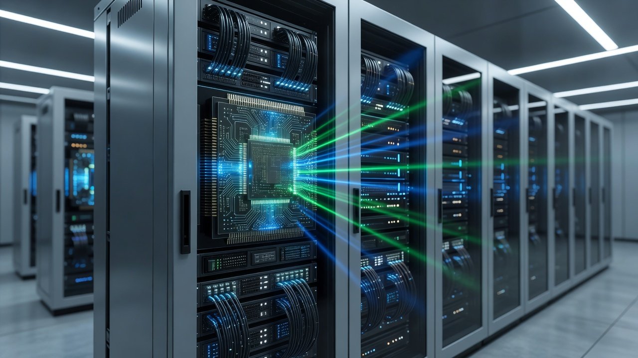
Optical computing chips are transforming enterprise AI by leveraging light instead of electrons for data processing. In 2026, these chips deliver substantial improvements in energy efficiency and speed for large-scale AI workloads compared to traditional GPUs and electronic processors. Enterprises across finance, healthcare, and logistics are deploying photonic accelerators to handle the exponential growth in model complexity and data volume. This technology promises to address the sustainability challenges of AI infrastructure while maintaining or exceeding performance levels. The shift toward optical solutions comes at a critical time when data centers face mounting pressure to reduce carbon footprints without sacrificing computational power. This article provides an in-depth comparison, detailed case studies, benchmarks, and actionable guidance for IT professionals evaluating these systems.
Key Comparisons: Optical Chips vs. GPUs and Electronic Chips
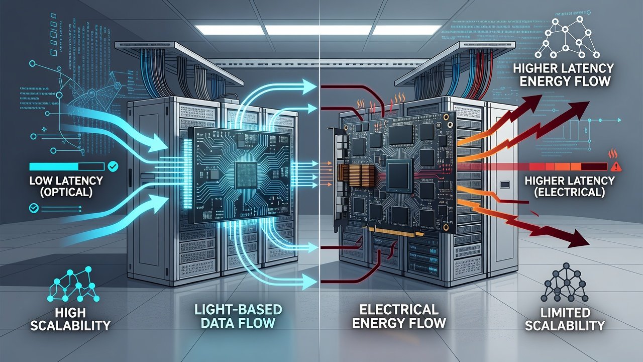
Optical computing excels in parallel processing tasks common to AI training and inference. Energy consumption drops significantly because photons generate less heat than electrons during transmission. Latency reductions occur due to faster light-based signal transmission across data center interconnects, bypassing many electrical bottlenecks. Scalability improves as optical systems handle higher bandwidth without proportional power increases or additional cooling infrastructure. These advantages become especially pronounced in workloads involving large matrix operations typical of deep learning frameworks.
Energy Savings Analysis
Deployments show optical chips reducing power usage by up to 70% for matrix multiplications in neural networks. This efficiency supports sustainable data center operations amid rising AI demands. The U.S. Department of Energy highlights photonic approaches as key to lowering overall IT energy footprints through reduced thermal output and optimized light routing. In contrast, GPU clusters often require dedicated power substations and advanced liquid cooling to manage heat dissipation from dense electronic components.
Latency and Scalability Benefits
Latency improvements reach 40-60% in inference pipelines when optical interconnects replace copper-based links. Scalability allows clusters to expand without thermal throttling issues common in GPU setups. Benchmarks from early 2026 adopters demonstrate consistent performance at scale, with optical systems maintaining throughput even as node counts increase beyond traditional electronic limits. The National Institute of Standards and Technology continues to publish standards supporting these photonic interfaces for reliable enterprise integration.
Enterprise Case Studies and Performance Benchmarks
Several Fortune 500 companies piloted optical solutions in 2025-2026. A major financial services firm reported 3x faster model training times alongside 55% lower cooling costs when migrating credit risk models to optical accelerators. The deployment involved hybrid setups where optical cores handled convolutional layers while electronic processors managed sequential decision trees. A healthcare AI provider achieved 48% latency cuts in real-time diagnostics workloads, enabling faster patient outcome predictions across distributed hospital networks. ROI was realized within 14 months through reduced electricity bills and higher utilization rates of existing server racks.
Another logistics enterprise integrated optical accelerators for supply chain optimization, noting 65% energy savings and improved throughput during peak seasons. Their system processed real-time sensor data from global fleets using photonic matrix operations, resulting in more accurate demand forecasting. A fourth case from a media streaming company showed optical chips reducing inference latency by 52% for recommendation engines, allowing personalized content delivery at higher volumes without expanding physical infrastructure. These metrics underscore the technology's edge in high-volume AI environments where both performance and sustainability matter equally.
Practical Integration Steps for IT Teams
Successful adoption requires methodical planning. First, assess current AI workloads to identify photonics-compatible tasks such as convolutional neural networks or transformer attention mechanisms. Second, partner with vendors offering hybrid optical-electronic systems for gradual migration that avoids full rip-and-replace strategies. Third, upgrade interconnect fabrics to support optical I/O standards while ensuring backward compatibility with existing Ethernet or InfiniBand networks. Fourth, conduct pilot tests measuring energy, latency, and accuracy against GPU baselines over at least three months of representative workloads. Fifth, train staff on photonic-specific optimization techniques including light routing algorithms and wavelength management. Sixth, establish monitoring dashboards that track photonic metrics alongside traditional CPU and GPU utilization. Seventh, develop fallback procedures to revert to electronic processing during any initial stability issues. Following these steps minimizes disruption while maximizing efficiency gains across the organization.
Common Adoption Challenges and Solutions
Integration hurdles include compatibility with legacy software stacks and the learning curve for new hardware abstractions. Solutions involve middleware layers that abstract optical operations into familiar CUDA-like APIs, allowing developers to port code with minimal changes. Data center retrofits for optical cabling require careful planning to avoid downtime; phased installations during maintenance windows have proven effective. Another challenge involves skill gaps among engineering teams accustomed to electronic architectures. Companies address this through vendor-led workshops and certification programs focused on photonic design principles. Supply chain considerations also arise, as specialized optical components may have longer lead times than standard GPUs. Mitigation strategies include maintaining buffer inventories and diversifying supplier relationships early in the planning phase.
How Optical Computing Enhances Specific AI Workloads
Beyond general metrics, optical chips particularly benefit computer vision tasks where massive parallel convolutions dominate. Natural language processing models see gains in embedding generation and attention computations due to high-bandwidth optical pathways. Recommendation systems in e-commerce leverage the low-latency inference to serve millions of users simultaneously. Scientific simulations involving large matrix factorizations also demonstrate strong results when ported to photonic hardware.
Decision Framework for Adoption
- Evaluate workload profiles for parallelism intensity and data movement patterns.
- Calculate total cost of ownership including power, cooling, and maintenance over a three-year horizon.
- Review vendor roadmaps for future optical chip generations and software ecosystem maturity.
- Assess risk tolerance for early-adopter challenges versus potential competitive advantages.
- Consult with facilities teams on power and space implications before procurement.
Frequently Asked Questions
How do optical chips handle mixed AI workloads?
Hybrid architectures combine optical cores for parallel computations with electronic controls for sequential tasks, delivering balanced performance across diverse model types.
What ROI timelines are typical?
Enterprises often see payback within 12-18 months via energy and operational savings, based on 2026 deployments across multiple industries.
Are optical solutions ready for production use?
Yes, multiple vendors now offer commercial-grade chips with enterprise support and proven benchmarks in live environments at scale.
Can optical chips integrate with existing GPU clusters?
Most implementations use hybrid configurations where optical accelerators complement rather than replace GPUs for specific pipeline stages.
What skill sets are needed for maintenance?
Teams benefit from knowledge in photonics, basic optics troubleshooting, and updated monitoring tools alongside traditional IT expertise.
How does this technology impact sustainability goals?
Significant reductions in energy consumption directly support corporate net-zero targets and regulatory compliance for data center emissions.
Conclusion
Optical computing chips represent a pivotal advancement for 2026 AI efficiency. By focusing on energy savings, latency reductions, and scalable designs, enterprises can achieve meaningful competitive advantages while advancing sustainability objectives. IT teams should begin evaluations now to stay ahead in this rapidly evolving field and position their organizations for future growth in AI capabilities.

No comments yet. Be the first!